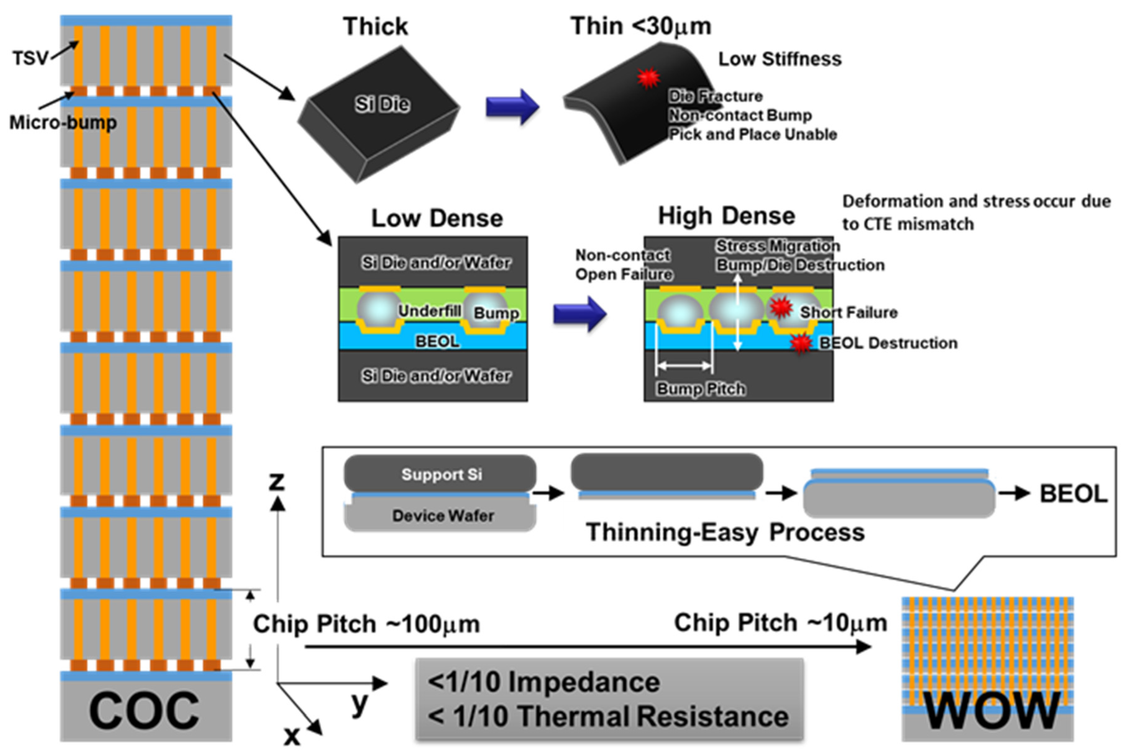
Schematic of the chip/bump build-up cross-section.
4.6 (610) · $ 27.50 · In stock


Hybrid Bonding Process Flow - Advanced Packaging Part 5
Levels and Steps of Integration. Introduction, by Suny Li

Thermal copper pillar bump - Wikipedia

a) Schematic of 3-D stack package. (b) Cross section of 3-D stack
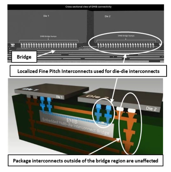
Intel's EMIB Packaging Technology – A Deep Dive - SemiWiki

Zhuojie WU Research profile

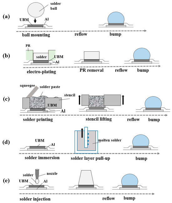
Maxim Wafer-Level Package Assembly Guide

PDF) Understanding and Improving Reliability for Wafer Level Chip

Polymers in Electronic Packaging: Build-Up Films for Flip Chip
What Are Through-Silicon Vias?
Weibull plots for TCoB fails based 1000 ohms and 0.1 ohms
Electronics, Free Full-Text

Schematic structures of the cross-section of the indium bump just
Materials, Free Full-Text
Schematic of the chip/bump build-up cross-section.