- Home
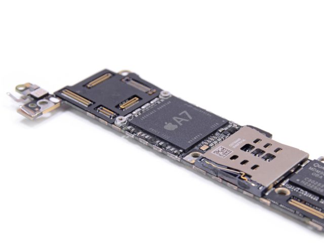
- chip pad
- pcb - Connecting pads with the same functionality belonging to one chip - Electrical Engineering Stack Exchange
pcb - Connecting pads with the same functionality belonging to one chip - Electrical Engineering Stack Exchange
4.8 (496) · $ 18.50 · In stock

I have a question about routing style of pads with the same functionality belonging to one chip. I draw a picture in Paint (fictional IC; let it be the SOIC8 footprint). GND is only as example (it
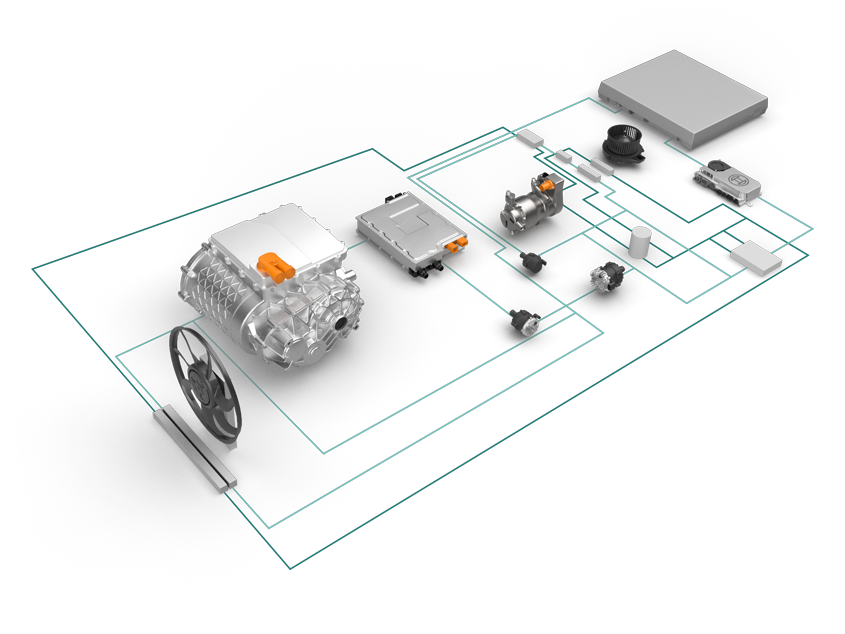
Thermal management for hybrid systems and electric drives

I'm trying to build a clock, rate my first schematic design - Project Guidance - Arduino Forum
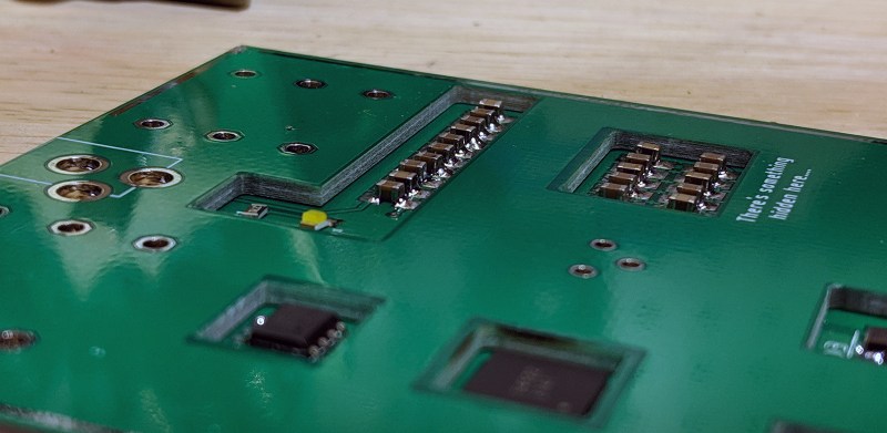
Oreo Construction: Hiding Your Components Inside The PCB

pcb design - PCB Layout. The path between pads - Electrical Engineering Stack Exchange
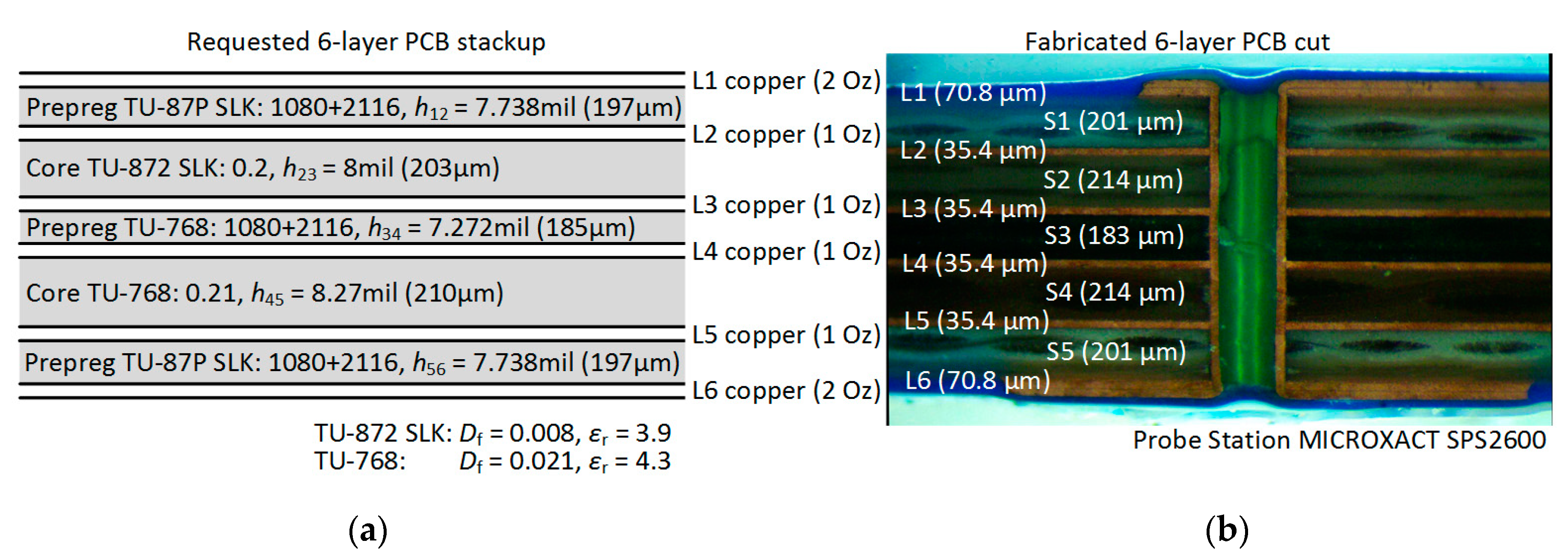
Symmetry, Free Full-Text

Unlocking PCB Reverse Engineering: Techniques, Benefits

High-Bandwidth Memory (HBM) - Semiconductor Engineering
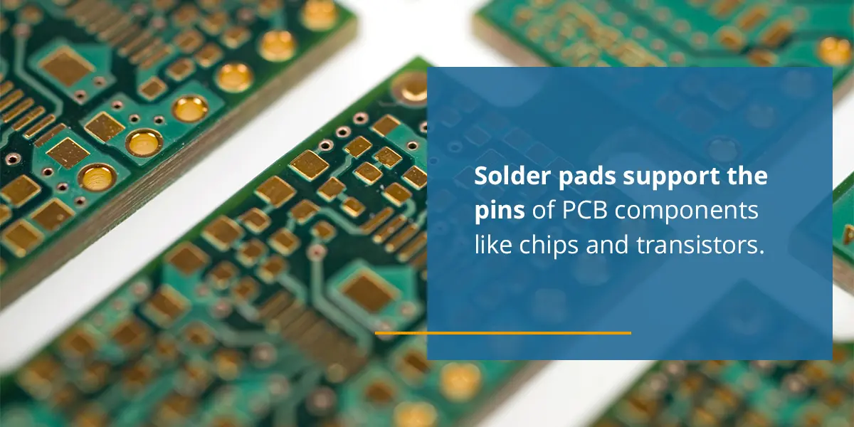
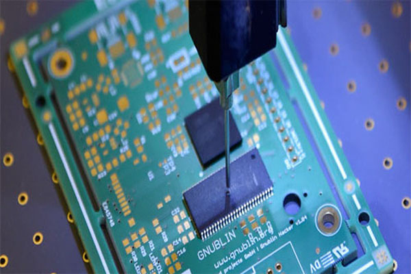
To Design for PCB Assembly

Reducing Noise in an SMPS Through Layout and Filtering - Technical Articles
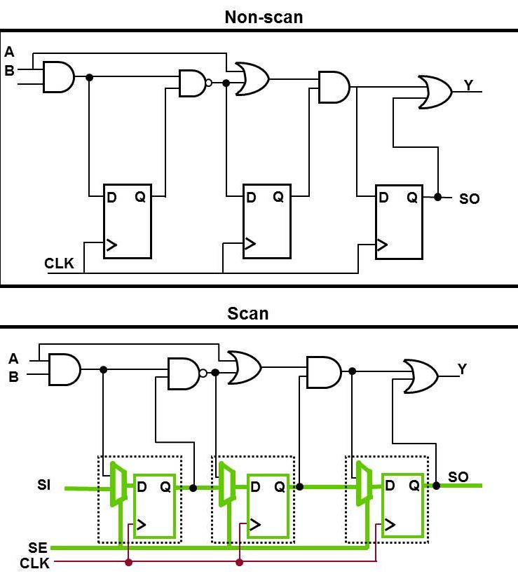
Scan Test - Semiconductor Engineering
PCB Design & Manufacturing

Electrical variation and reliability results for array structure for
What is a pad stack in PCB? - Quora